Global Polymer Capacitor Market Set to Reach USD 3.95 Billion by 2032, Driven by Consumer Electronics and 5G Expansion
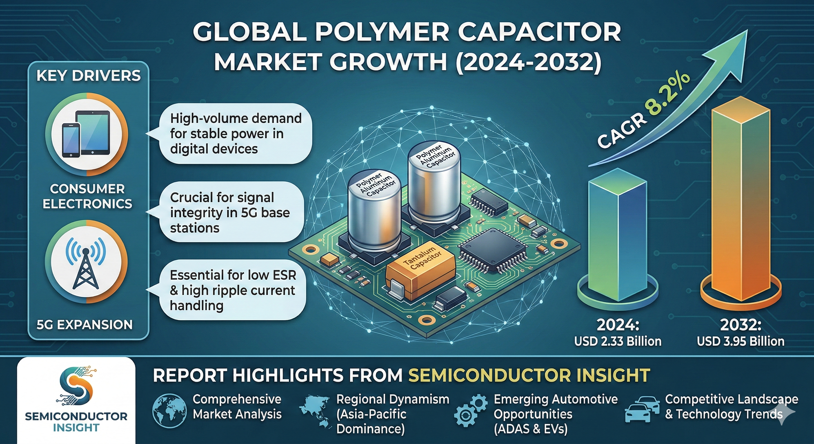
The global Polymer Capacitor Market, valued at USD 2.33 billion in 2024, is on a trajectory of significant expansion, projected to reach USD 3.95 billion by 2032. This growth, representing a compound annual growth rate (CAGR) of 8.2%, is detailed in a comprehensive new report published by Semiconductor Insight. The study highlights the critical role of these advanced electronic components in ensuring stable power delivery and signal integrity across a vast spectrum of modern technologies, particularly in the high-volume consumer electronics sector.
Polymer capacitors, essential for smoothing voltage and filtering noise in high-frequency circuits, are becoming indispensable for modern electronic design. Their superior electrical characteristics, including low equivalent series resistance (ESR) and high ripple current handling, make them a cornerstone of digital devices, from the smartphone in your pocket to the sophisticated servers powering the cloud. These components are increasingly favored over traditional alternatives because they offer enhanced performance and reliability in increasingly compact and power-hungry devices. Their robustness and long operational life are key factors driving their adoption in applications where failure is not an option.
Consumer Electronics Proliferation: The Primary Growth Engine
The report identifies the relentless global demand for consumer electronics as the paramount driver for polymer capacitor growth. With this segment accounting for the largest share of global demand, the correlation between consumer device shipments and capacitor consumption is direct and substantial. The global consumer electronics market itself continues to see billions of units shipped annually, fueling consistent, high-volume demand for these critical components.
"The massive concentration of electronics manufacturing and original equipment manufacturers (OEMs) in the Asia-Pacific region, which is the dominant consumer and producer, is a key factor in the market's dynamism," the report states. With the proliferation of features like 5G connectivity, high-resolution displays, and advanced mobile computing, the need for stable, efficient power management solutions is set to intensify, especially as processing speeds increase and device form factors shrink.
Download FREE Sample Report:
Polymer Capacitor Market - View in Detailed Research Report
Market Segmentation: Polymer Aluminum Capacitors and Consumer Applications Dominate
The report provides a detailed segmentation analysis, offering a clear view of the market structure and key growth segments:
Segment Analysis:
By Type
Polymer Tantalum Electrolytic Capacitor
Polymer Aluminum Electrolytic Capacitor
Others (Hybrid and Niobium)
By Application
Consumer Electronics
Automotive
Industrial
Others
Telecommunications Infrastructure
Power Supplies
Computing Hardware
Others
By End User
Original Equipment Manufacturers (OEMs)
Electronic Manufacturing Services (EMS)
Aftermarket/Component Distributors
Get Full Report Here:
Polymer Capacitor Market, Global Business Strategies 2025-2032 - View in Detailed Research Report
Competitive Landscape: Key Players and Strategic Focus
The report profiles key industry players, including:
Murata Manufacturing Co., Ltd.
Nichicon Corporation
Panasonic Corporation
KEMET (Yageo Corporation)
Nippon Chemi-Con (NCC)
Rubycon Corporation
AVX Corporation (Kyocera Group)
Vishay Intertechnology, Inc.
TDK Corporation
Apaq Technology Co., Ltd.
Lelon Electronics Corp.
Jianghai Capacitor
Aihua Group
Illinois Capacitor, Inc.
Shenzhen Maxking Electronics Co., Ltd.
These companies are focusing on technological advancements, such as developing capacitors with higher capacitance density and improved thermal stability, and geographic expansion into high-growth regions to capitalize on emerging opportunities.
Emerging Opportunities in Automotive and 5G Infrastructure
Beyond traditional drivers, the report outlines significant emerging opportunities. The rapid electrification of the automotive industry, particularly the expansion of Advanced Driver Assistance Systems (ADAS) and electric vehicle powertrains, presents new growth avenues, requiring robust and reliable capacitors for safety-critical and high-power applications. Furthermore, the global rollout of 5G networks is a major trend. Polymer capacitors are essential in 5G base stations and network equipment, creating sustained demand from this high-growth sector.
Report Scope and Availability
The market research report offers a comprehensive analysis of the global and regional Polymer Capacitor markets from 2025–2032. It provides detailed segmentation, market size forecasts, competitive intelligence, technology trends, and an evaluation of key market dynamics.
For a detailed analysis of market drivers, restraints, opportunities, and the competitive strategies of key players, access the complete report.
Read Full Report:
https://semiconductorinsight.com/download-sample-report/?product_id=122478
Download Sample Report:
https://semiconductorinsight.com/
Other Related Reports:
Light Sources for Lithography Market
Quantum Chip Market
Global Radio Frequency and Microwave Filter Market
India Optical Component Market
Global Multi-mode Receiver (MMR) Market
Silicon Quantum Dot Market
Optical Detection Biosensors Market
Global Desktop USB Port Chargers Market
NDIR (Non-Dispersive Infrared) Gas Sensors Market
Electric Vehicle Hall Current Sensors Market
About Semiconductor Insight
Semiconductor Insight is a leading provider of market intelligence and strategic consulting for the global semiconductor and high-technology industries. Our in-depth reports and analysis offer actionable insights to help businesses navigate complex market dynamics, identify growth opportunities, and make informed decisions. We are committed to delivering high-quality, data-driven research to our clients worldwide.
Website:
https://semiconductorinsight.com/
International: +91 8087 99 2013
LinkedIn: Follow Us
#PolymerCapacitors #SemiconductorIndustry #ElectronicsManufacturing #5GTechnology #EVInnovation #TechTrends2032 #ConsumerElectronics #PassiveComponents #MarketResearch #EnergyEfficiency #TechGrowth
Global Polymer Capacitor Market Set to Reach USD 3.95 Billion by 2032, Driven by Consumer Electronics and 5G Expansion
The global Polymer Capacitor Market, valued at USD 2.33 billion in 2024, is on a trajectory of significant expansion, projected to reach USD 3.95 billion by 2032. This growth, representing a compound annual growth rate (CAGR) of 8.2%, is detailed in a comprehensive new report published by Semiconductor Insight. The study highlights the critical role of these advanced electronic components in ensuring stable power delivery and signal integrity across a vast spectrum of modern technologies, particularly in the high-volume consumer electronics sector.
Polymer capacitors, essential for smoothing voltage and filtering noise in high-frequency circuits, are becoming indispensable for modern electronic design. Their superior electrical characteristics, including low equivalent series resistance (ESR) and high ripple current handling, make them a cornerstone of digital devices, from the smartphone in your pocket to the sophisticated servers powering the cloud. These components are increasingly favored over traditional alternatives because they offer enhanced performance and reliability in increasingly compact and power-hungry devices. Their robustness and long operational life are key factors driving their adoption in applications where failure is not an option.
Consumer Electronics Proliferation: The Primary Growth Engine
The report identifies the relentless global demand for consumer electronics as the paramount driver for polymer capacitor growth. With this segment accounting for the largest share of global demand, the correlation between consumer device shipments and capacitor consumption is direct and substantial. The global consumer electronics market itself continues to see billions of units shipped annually, fueling consistent, high-volume demand for these critical components.
"The massive concentration of electronics manufacturing and original equipment manufacturers (OEMs) in the Asia-Pacific region, which is the dominant consumer and producer, is a key factor in the market's dynamism," the report states. With the proliferation of features like 5G connectivity, high-resolution displays, and advanced mobile computing, the need for stable, efficient power management solutions is set to intensify, especially as processing speeds increase and device form factors shrink.
Download FREE Sample Report:
Polymer Capacitor Market - View in Detailed Research Report
Market Segmentation: Polymer Aluminum Capacitors and Consumer Applications Dominate
The report provides a detailed segmentation analysis, offering a clear view of the market structure and key growth segments:
Segment Analysis:
By Type
Polymer Tantalum Electrolytic Capacitor
Polymer Aluminum Electrolytic Capacitor
Others (Hybrid and Niobium)
By Application
Consumer Electronics
Automotive
Industrial
Others
Telecommunications Infrastructure
Power Supplies
Computing Hardware
Others
By End User
Original Equipment Manufacturers (OEMs)
Electronic Manufacturing Services (EMS)
Aftermarket/Component Distributors
Get Full Report Here:
Polymer Capacitor Market, Global Business Strategies 2025-2032 - View in Detailed Research Report
Competitive Landscape: Key Players and Strategic Focus
The report profiles key industry players, including:
Murata Manufacturing Co., Ltd.
Nichicon Corporation
Panasonic Corporation
KEMET (Yageo Corporation)
Nippon Chemi-Con (NCC)
Rubycon Corporation
AVX Corporation (Kyocera Group)
Vishay Intertechnology, Inc.
TDK Corporation
Apaq Technology Co., Ltd.
Lelon Electronics Corp.
Jianghai Capacitor
Aihua Group
Illinois Capacitor, Inc.
Shenzhen Maxking Electronics Co., Ltd.
These companies are focusing on technological advancements, such as developing capacitors with higher capacitance density and improved thermal stability, and geographic expansion into high-growth regions to capitalize on emerging opportunities.
Emerging Opportunities in Automotive and 5G Infrastructure
Beyond traditional drivers, the report outlines significant emerging opportunities. The rapid electrification of the automotive industry, particularly the expansion of Advanced Driver Assistance Systems (ADAS) and electric vehicle powertrains, presents new growth avenues, requiring robust and reliable capacitors for safety-critical and high-power applications. Furthermore, the global rollout of 5G networks is a major trend. Polymer capacitors are essential in 5G base stations and network equipment, creating sustained demand from this high-growth sector.
Report Scope and Availability
The market research report offers a comprehensive analysis of the global and regional Polymer Capacitor markets from 2025–2032. It provides detailed segmentation, market size forecasts, competitive intelligence, technology trends, and an evaluation of key market dynamics.
For a detailed analysis of market drivers, restraints, opportunities, and the competitive strategies of key players, access the complete report.
Read Full Report: https://semiconductorinsight.com/download-sample-report/?product_id=122478
Download Sample Report: https://semiconductorinsight.com/
Other Related Reports:
Light Sources for Lithography Market
Quantum Chip Market
Global Radio Frequency and Microwave Filter Market
India Optical Component Market
Global Multi-mode Receiver (MMR) Market
Silicon Quantum Dot Market
Optical Detection Biosensors Market
Global Desktop USB Port Chargers Market
NDIR (Non-Dispersive Infrared) Gas Sensors Market
Electric Vehicle Hall Current Sensors Market
About Semiconductor Insight
Semiconductor Insight is a leading provider of market intelligence and strategic consulting for the global semiconductor and high-technology industries. Our in-depth reports and analysis offer actionable insights to help businesses navigate complex market dynamics, identify growth opportunities, and make informed decisions. We are committed to delivering high-quality, data-driven research to our clients worldwide.
🌐 Website: https://semiconductorinsight.com/
📞 International: +91 8087 99 2013
🔗 LinkedIn: Follow Us
#PolymerCapacitors #SemiconductorIndustry #ElectronicsManufacturing #5GTechnology #EVInnovation #TechTrends2032 #ConsumerElectronics #PassiveComponents #MarketResearch #EnergyEfficiency #TechGrowth